- 您现在的位置:买卖IC网 > Sheet目录1992 > DAC5674IPHPG4 (Texas Instruments)IC DAC 14BIT 400MSPS 48-HTQFP
DAC5674
SLWS148A SEPTEMBER 2003 REVISED OCTOBER 2005
www.ti.com
7
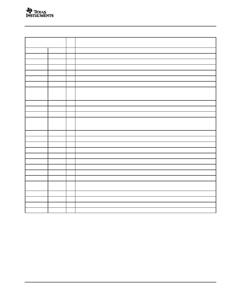
Terminal Functions
TERMINAL
I/O
DESCRIPTION
NAME
NO.
I/O
DESCRIPTION
AGND
37, 41, 44
I
Analog ground return
AVDD
45, 46
I
Analog supply voltage
BIASJ
40
O
Full-scale output current bias
CLK
29
I
External clock input
CLKC
30
I
Complementary external clock input
CLKGND
31
I
Ground return for internal clock buffer
CLKVDD
32
I
Internal clock buffer supply voltage
D[13..0]
316
I
Data bits 0 through 13
D13 is most significant data bit (MSB)
D0 is least significant data bit (MSB)
DIV[1..0]
27,28
I
PLL prescaler divide ratio settings
DGND
1, 2, 19, 24
I
Digital ground return
DVDD
21, 47, 48
I
Digital supply voltage
EXTIO
39
I/O
Used as external reference input when internal reference is disabled (i.e., EXTLO connected to AVDD).
Used as internal reference output when EXTLO = AGND, requires a 0.1-
F decoupling capacitor to AGND
when used as reference output
EXTLO
38
I
For internal reference connect to AGND. Connect to AVDD to disable the internal reference
HP1
17
I
Filter 1 high-pass setting. Active high
HP2
18
I
Filter 2 high-pass setting. Active high
IOGND
20
I
Input digital ground return
IODVDD
22
I
Input digital supply voltage
IOUT1
43
O
DAC current output. Full scale when all input bits are set 1
IOUT2
42
O
DAC complementary current output. Full scale when all input bits are 0
LPF
35
I
PLL loop filter connection
PLLGND
33
I
Ground return for internal PLL
PLLLOCK
25
O
PLL lock status bit. PLL is locked to input clock when high. Provides output clock equal to the data rate
when the PLL is disabled.
PLLVDD
34
I
Internal PLL supply voltage. Connect to PLLGND to disable PLL clock multiplier.
RESET
26
I
Reset internal registers. Active high
SLEEP
36
I
Asynchronous hardware power-down input. Active high. Internally pull down.
X4
23
I
4
× interpolation mode. Active high. Filter 1 is bypassed when connected to DGND
发布紧急采购,3分钟左右您将得到回复。
相关PDF资料
DAC7621EBG4
IC SNGL 12BIT PARALLEL D/A 20SSO
DAC7801KPG4
IC DUAL 12BIT CMOS DAC 24-DIP
DAC8043AESZ
IC DAC 12BIT MULT SRL INP 8SOIC
DAC8043GP
IC DAC 12BIT MULTIPLY CMOS 8-DIP
DAC8221GP
IC DAC 12BIT DUAL W/BUFF 24-DIP
DAC8222GPZ
IC DAC 12BIT DUAL W/BUFF 24DIP
DAC8229FSZ-REEL
IC DAC 8BIT DUAL V-OUT 20SOIC
DAC8248FS
IC DAC 12BIT DUAL W/BUFF 24-SOIC
相关代理商/技术参数
DAC5674IPHP-ND
制造商: 功能描述: 制造商:undefined 功能描述:
DAC5674IPHPR
功能描述:数模转换器- DAC 14-Bit 400 CommsDAC RoHS:否 制造商:Texas Instruments 转换器数量:1 DAC 输出端数量:1 转换速率:2 MSPs 分辨率:16 bit 接口类型:QSPI, SPI, Serial (3-Wire, Microwire) 稳定时间:1 us 最大工作温度:+ 85 C 安装风格:SMD/SMT 封装 / 箱体:SOIC-14 封装:Tube
DAC5674IPHPRG4
功能描述:数模转换器- DAC 14-Bit 400 CommsDAC RoHS:否 制造商:Texas Instruments 转换器数量:1 DAC 输出端数量:1 转换速率:2 MSPs 分辨率:16 bit 接口类型:QSPI, SPI, Serial (3-Wire, Microwire) 稳定时间:1 us 最大工作温度:+ 85 C 安装风格:SMD/SMT 封装 / 箱体:SOIC-14 封装:Tube
DAC5675
制造商:TI 制造商全称:Texas Instruments 功能描述:14-BIT, 400-MSPS DIGITAL-TO-ANALOG CONVERTER
DAC5675A
制造商:TI 制造商全称:Texas Instruments 功能描述:14-Bit, 400MSPS Digital-to-Analog Converter
DAC5675AEVM
功能描述:数据转换 IC 开发工具 DAC5675A Eval Mod RoHS:否 制造商:Texas Instruments 产品:Demonstration Kits 类型:ADC 工具用于评估:ADS130E08 接口类型:SPI 工作电源电压:- 6 V to + 6 V
DAC5675AIPHP
功能描述:数模转换器- DAC 14-Bit 400-MSPS RoHS:否 制造商:Texas Instruments 转换器数量:1 DAC 输出端数量:1 转换速率:2 MSPs 分辨率:16 bit 接口类型:QSPI, SPI, Serial (3-Wire, Microwire) 稳定时间:1 us 最大工作温度:+ 85 C 安装风格:SMD/SMT 封装 / 箱体:SOIC-14 封装:Tube
DAC5675AIPHP
制造商:Texas Instruments 功能描述:IC DAC 14BIT 400MSPS 48-HTQFP